Design rules
-
PCB manufactures have certain requirements that the design must follow to be manufacturable without problems.
-
JLCPCB has requirements on this page: https://jlcpcb.com/capabilities/Capabilities
-
-
PCB design software can usually check the requirements during component placement and routing. Requirements can also be manually checked with DRC (design rules check).
-
Design rules should be changed in the design software based on the manufacturer’s requirements/capabilities before starting PCB layout.
Layers
It’s recommended to use 4 layers:
-
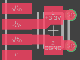
Signals and power (top)
-
GND
-
GND
-
Signals and power (bottom)
General steps
-
Start with initial component placement. Majority of time should be spent in this step to make routing the signals easier.
-
Route the signals and connect power and ground with vias to internal layers. Adjust component placement where necessary to make room for vias and tracks or to bring components closer to each other.
-
Create power and ground copper areas on internal layers. It’s also useful to add ground copper areas on top and bottom layers for better thermal performance.
Component placement
-
Use airwires to find good location and orientation for components.
-
Try to make airwires as short as possible to have short tracks.
-
Find signals that are crossing each other. Then swap the pins on the schematic if possible or adjust the components placement or move components to bottom layer. It’s easier to route the signals if tracks are not crossing each other.
-
-
Place larger components first and then place smaller components next to the larger ones.
-
For example place microcontroller first and then place decoupling capacitors next to the pins. Then place resistors close to the microcontroller.
-
Decoupling capacitors
-
Place decoupling capacitors as close as possible to power pins.
-
This reduces the noise that could picked up on the longer track.
-
Shorter tracks also resist the current flow less.
-
-
Connect power and ground with vias.
-
Avoid placing vias between component pins and decoupling capacitor.
-
Current should flow from power supply to capacitor and from decoupling capacitor to the component.
-
When tha components are hand soldered, then it’s fine to place the vias inside the capacitor’s pads.
-
When reflow soldering, vias would need to be plugged/filled first to avoid solder paste flowing into the via holes.
-
ESD protection
Place ESD protection components as close to the connector as possible.
Routing
Track widths
-
Current carrying capability should be considered when choosing the width for a track.
-
Wider tracks have less resistance and can carry more current.
-
Calculators can be used to calculate track widths and other properties:
-
Wider tracks are also mechanically more robust, which can be useful when doing hand soldering or rework.
-
Vias
-
Via size can be calculated by current capability.
-
Multiple smaller vias can be used in parallel instead of one larger via.
-
Calculators can be used to calculate via properties:
-
Current return paths
-
Current return paths should be considered when placing components and routing tracks.
-
Current tends to flow through the path of least impedance.
-
Electrical impedance is a combination of resistance, capacitive reactance and inductive reactance.
-
-
At low frequencies current flows through the shortest (least resistance) path.
-
With higher frequencies, more return current will flow underneath the track on the path of least impedance.
-
For example if the track is on the first layer, and the ground area is on the second layer, then at higher frequencies the return current tends to flow through the ground area below the track on the first layer.
-
-
Area enclosed with forward and return current is called current loop.
-
Larger current loops create more noise.
-
Loop area should be minimized by placing components close to each other, using short tracks and making sure the return current can flow through the path of least impedance.
-
More information:
Copper areas
-
Copper areas (polygon pour) can be used to connect nets (ground, power, motor driver outputs) that carry higher currents.
-
Avoid creating large gaps in ground planes by placing vias close to each other.
-
Current has to flow around the gaps which can create larger current loops.
-
Thermal pads
Connect thermal pads to the ground copper areas with multiple vias.