Electronics design checklist
- Repository
- General
- Use components available in the lab or in storage
- Make sure that the capacitor voltage rating is higher than the supply voltage
- Use capacitors in a larger package for higher capacitance and higher voltage rating
- Keep LED current low
- Connect LED with correct polarity
- Use switching regulator for servos
- Do not use 5 V LDO linear regulator if switching regulator is used
- Make sure that all footprints have 3D model in Altium Designer
- Schematic
- Avoid overlapping schematic objects
- Align schematic objects to default grid size
- Use correct component designators
- Make sure component product names are correct and visible
- Fix all ERC errors or warnings
- Order connector symbol pins by pin numbers
- Avoid grouping microcontroller pins by their usage in the schematic
- Use consistent passive component values and units
- Name differential pairs with correct suffix
- Use different net names at the isolated sides
- Make sure that the symbol pin and footprint pad designators match
- Use same connector pinouts as on the test mainboard
- Make sure that microcontroller reset pin has a capacitor connected to it
- Use consistent microcontroller timer channel assignment for encoders
- Do not use the same microcontroller timer for both encoder mode and for generating PWM
- Make sure that all necessary signals go through the isolator
- Make sure that signals match on different sides of the isolator
- Connect IS471FE output signal to 5V tolerant pin
- Connect DRV8243 thermal pad to GND
- Avoid using the highest DRV8243 output slew rates
- Use DRV8243 in PH/EN mode
- Connect all DRV8243 nSLEEP pins to single microcontroller pin
- Configure TPS62933 switching frequency based on the inductor value
- PCB layout
- Set design rules by PCB manufacturer’s capabilities
- Do not set clearance rules to the lowest value allowed by the PCB manufacturer
- Do not use via sizes that increase PCB cost
- Use direct connection for copper polygons by default
- Avoid acute angles
- Create Board Outline Clearance rule in Altium Designer
- Fix all DRC errors or warnings
- Use 4-layer PCB stackup
- No copper should be below isolator
- Connect USB connector shield to copper polygon and with vias to other layers for mechanical durability
- Place decoupling capacitors as close as possible to power pins
- Place physically smaller capacitors closer to component’s power input pins
- Take into account the size of the plugs that connect to the connectors on the PCB
- Make sure that USB connector is placed over the edge of PCB to clear the flanges
- Keep track short and straight
- Avoid routing GND with long tracks
- Avoid routing tracks close to each other to reduce crosstalk
- Keep enough clearance between same net copper
- Prefer small vias to large vias
- Do not flood fill signal layers with GND copper
- Avoid dead copper
- Place ESD protection close to the source of the ESD
- Make sure that pin 1 indicator is on the component footprint
- Add mounting holes
- Follow TPS62933 layout guidelines
- Avoid putting silkscreen test below components
- Number encoder connectors and motor drivers on the silkscreen
- Altium Designer specific
- Generate Gerber X2 files when the design is completed
Repository
Add all necessary files
All project files that are necessary to open the project should be added to the repository. All symbols and footprint should be local to the project and included in the repository.
Main files are included below.
-
Altium Designer
-
*.PrjPcb- project file -
*.SchDoc- schematic sheet -
*.SchLib- component symbols -
*.PcbLib- component footprints -
*.PcbDoc- PCB layout -
*.BomDoc- BOM (Bill of Materials) -
*.OutJob- Output Jobs (for example generating Gerber X2 files for fabricating PCBs)
-
-
KiCad
-
*.kicad_pro- project file -
*.kicad_sch- schematic sheet -
*.kicad_sym- component symbols -
*.pretty/*.kicad_mod- component footprints -
*.kicad_pcb- PCB layout
-
General
Use components available in the lab or in storage
-
List of components in the storage is on the Components page.
-
Most of the capacitors and resistors are available in the lab.
Make sure that the capacitor voltage rating is higher than the supply voltage
-
Higher voltage than the capacitor’s rated voltage can damage the capacitor.
-
Class 2 ceramic capacitor’s effective capacitance decreases with DC bias.
Use capacitors in a larger package for higher capacitance and higher voltage rating
-
Higher capacitance and voltage rating in a smaller package usually makes the capacitor more expensive.
-
Or the capacitor just might not exist.
Keep LED current low
-
Choose LED current limit resistor value so that the LED is not too bright.
-
Current of 0.1 to 0.2 A is usually enough for the LED to be visible, but not blinding.
-
When calculating the resistor value, be mindful that the LED’s forward voltage decreased with lower current. It’s usually shown on the
Forward Current vs Forward Voltagegraph in the datasheet.
-
Connect LED with correct polarity
-
LEDs emit light when the current flows through them, which does not happen when the LED is reverse-biased.
Use switching regulator for servos
-
Servos used in the course can draw up to about 1 A of current.
-
Linear regulators are inefficient with large input and output voltage difference and high current output. This results in a lot of wasted power and heat being generated.
-
Simplified example:
-
Input voltage: 16 V
-
Output voltage: 5 V
-
Output current: 2 A ( 2 servos)
-
Wasted power:
(16 V - 5 V) * 2 A = 11 V * 2A = 22 W -
Average current is lower than 2 A, but it is a good practice to design for worst case conditions.
-
-
Schematic
Avoid overlapping schematic objects
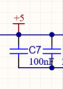
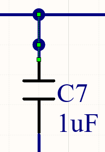
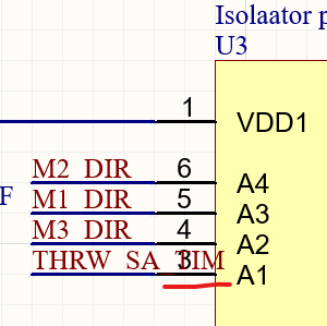
Overlapping schematic objects can reduce readability and in some cases in some cases result in unconnected signals.
Examples
Align schematic objects to default grid size
-
Altium Designer defaults to 100 mil grid and KiCad to 50 mil grid.
-
Default grid size on schematic sheets should not be changed to avoid misaligned symbols causing wires to be disconnected.
-
Symbols should be designed so that pin’s connection/attachment point (hotspot) is aligned with the grid.
Use correct component designators
-
Component designators are usually a combination of letters and numbers.
-
Examples: R1, C15, U2
-
-
Use standard or commonly used designators.
-
Avoid using different designator letters for same type of component.
Make sure component product names are correct and visible
-
Component product names are usually shown below or near the symbol.
-
Product name does not need to be shown for generic components (resistors, capacitors).
Fix all ERC errors or warnings
-
All errors and warnings should be properly fixed.
-
Errors and warning should not be suppressed/hidden.
Order connector symbol pins by pin numbers
-
Not having pins in sequential order makes the schematic harder to read.
Avoid grouping microcontroller pins by their usage in the schematic
-
Symbols should not be made specific to the project demands.
-
Symbol should be generic enough to work in different projects, where pins are used in different ways.
-
Changing pin assignments should not require the symbol to be changed.
-
Microcontroller pins can be ordered and grouped by the pin name.
Use consistent passive component values and units
-
For example, use either 100n, 100nF, 0.1u or 0.1uF, but stick to a single value and unit combination.
Name differential pairs with correct suffix
-
Altium Designer uses
_Nand_Pby default. -
KiCad uses
+and-, orPandN.
Use different net names at the isolated sides
-
Using same net names would mean that the nets will be connected on the PCB.
-
For example, there is 5V from the USB on the microcontroller side and 5V on the motor drivers side.
Make sure that the symbol pin and footprint pad designators match
-
Unmatched pads will not be connected to the correct nets on the PCB.
-
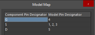
Altium Designer allows to have custom pin to pad mapping.
-
KiCad 10 allows to set pin number to multiple values.
-
For example:
[1-3]or[1,2,3] -
It is a replacement to pin stacking in previous version, but is not well documented.
-
https://forum.kicad.info/t/post-v9-new-features-and-development-news/58848/50
-
Use same connector pinouts as on the test mainboard
-
See: basketball-robot-guide/electronics/test-robot.adoc#_connector_pinouts
-
Motor, servo and ESC connectors should not be changed.
-
Having the same pinouts allows to easily swap between test mainboard and new mainboard.
Make sure that microcontroller reset pin has a capacitor connected to it
-
Check microcontroller datasheet for recommended value.
Use consistent microcontroller timer channel assignment for encoders
-
Connect ENCA to TIMx_CH1 and ENCB to TIMx_CH2.
-
Having encoders connected differently works, but needs to be handled in the firmware code.
Do not use the same microcontroller timer for both encoder mode and for generating PWM
-
Timers in encoder mode change the timer’s counter value, which messes up the PWM generation.
Make sure that all necessary signals go through the isolator
-
All signals for controlling the motors need to be connected through the isolators.
Make sure that signals match on different sides of the isolator
-
When connecting or changing the signals on one side the other side should be connected to match that.
Connect IS471FE output signal to 5V tolerant pin
-
Check microcontroller datasheet for 5V tolerant pins.
Avoid using the highest DRV8243 output slew rates
-
High slew rates have caused problems with motor not starting up properly.
-
Middle slew rates have worked fine.
Use DRV8243 in PH/EN mode
-
This simplifies microcontroller pin assignments as only one PWM per motor driver is needed.
PCB layout
Do not set clearance rules to the lowest value allowed by the PCB manufacturer
-
Having different nets close to each other increases crosstalk.
-
0.2 mm clearance is a good starting point.
-
Can be lowered if needed, but needs to comply with PCB manufacturer’s capabilities.
Do not use via sizes that increase PCB cost
-
Check
Min via hole size/diameterinformation here: https://cart.jlcpcb.com/quote
Use direct connection for copper polygons by default
-
Direct connection is better for higher currents since the connection resistance and inductance are lower, and thermal conductivity is better.
Avoid acute angles
-
Acute angles can complicate copper etching during PCB fabrication.
-
Altium Designer allows to create
Acute Anglerule, which simplifies finding acute angles.
Create Board Outline Clearance rule in Altium Designer
-
Altium Designer does not check for board outline clearance by default.
-
Make sure that clearance values comply with the PCB manufacturer’s capabilities.
Fix all DRC errors or warnings
-
All errors and warnings should be properly fixed.
-
Design rules should not be changed to fix the problems, if the rules to not comply with the PCB manufacturer’s capabilities.
-
Errors and warning should not be suppressed/hidden.
No copper should be below isolator
-
On all layers the isolation gap should be free of any copper (tracks, polygon) and other components to avoid making the gap narrower.
-
Make isolation gap as wide as the isolator body.
-
If mounting holes are placed in the isolation gap, make sure that mounting screws do not make the isolation gap narrower. Increase the width of the isolation gap around the mounting holes if necessary.
Connect USB connector shield to copper polygon and with vias to other layers for mechanical durability
-
Without additional copper the USB connector pads might be damaged when the USB cable bends the connector.
Place decoupling capacitors as close as possible to power pins
-
Longer connection has higher inductance, which reduces the effectiveness of the capacitor.
-
Making the connection wider also decreases the inductance.
-
Placing capacitors on the same layer as the main component usually result in a shorter connection and lower inductance compared to placing the capacitor on the opposite layer and connecting it with vias.
Place physically smaller capacitors closer to component’s power input pins
-
Capacitors in smaller package usually have lower inductance and are more effective compared to capacitors in larger package when placed closer to the component’s power pins.
Take into account the size of the plugs that connect to the connectors on the PCB
-
Micro-MaTch and microcontroller programmer plugs are wider than the connectors on the PCB.
-
Cables and wires on these plugs should also be taken into account to avoid the cables from colliding.
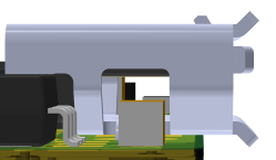
Make sure that USB connector is placed over the edge of PCB to clear the flanges
-
USB connector has flanges to make connecting the cable easier but the flange at the bottom can collide with the PCB.
Avoid routing GND with long tracks
-
Longer connection has higher inductance.
-
Use short tracks and vias near GND pads to connect to internal GND layers, which have lower inductance.
-
Vias can also be placed directly into pads.
Avoid routing tracks close to each other to reduce crosstalk
-
Crosstalk increases if tracks run close to each other.
-
Crosstalk also increases with distance. Crosstalk does not increase as much if only short segments of the tracks are close to each other.
Keep enough clearance between same net copper
-
Altium Designer and KiCad by default only check clearances between different nets.
-
Altium Designer allows to create rules to check same net clearance, but it is difficult to make it work in all cases.
Prefer small vias to large vias
-
It is possible to have more copper inside smaller vias on the same size PCB area.
-
This allows to carry more current and improve thermal conductivity.
-
-
Smaller vias inside a pad help against the solder flowing away from the pad, which can simplify soldering.
Do not flood fill signal layers with GND copper
-
In general, it can be a bad practice to simply flood fill signal layers with ground. It can create antennas which pick up and radiate noise and would need properly placed stitching vias to mitigate that. There is a solid ground on inner layers.
-
Using polygons where needed on outer layers for higher currents or for cooling the components is usually a better approach. Board edges and larger unused areas can be filled with ground polygons, but it’s better to avoid pouring over tracks.
-
Flood filling ground can also make it hard to notice when vias are not placed close to the GND pads, which makes the ground connection longer.
Relevant videos:
-
"Crosstalk on PCB layouts" by Texas Instruments
-
"You must Unlearn what You have Learned" by Eric Bogatin on Altium Academy channel.
Avoid dead copper
-
Unconnected/dead copper can increase the noise.
-
In Altium Designer make sure that
Remove Dead Copperis enabled in polygon properties. -
In KiCad make sure that
Remove islandsis set toAlwaysinCopper Zone Properties.
Place ESD protection close to the source of the ESD
-
Typical source for ESD is near the connectors.
-
ESD diodes should be placed close to the ESD source to avoid ESD propagating to other parts of the PCB.
-
Connect tracks from the connector first to the ESD diodes and from there to the other parts of the PCB.
-
Make GND connection between connector and ESD diodes short and wide for lower inductance, which increased the ESD protection effectiveness.
Make sure that pin 1 indicator is on the component footprint
-
Components that need to be soldered with correct orientation should have pin 1 indicator close to the pad 1.
Add mounting holes
-
Use at least 2 holes. 3 or 4 would be better.
-
Avoid large unsupported PCB overhangs. The PCB or the components can be damaged if the PCB is not supported well and bends too much.
-
Make sure that mounting screws and spacers do not collide with other components or short anything. Shorts might be also created if the fasteners scrape off the solder mask and contact the copper below.
-
Place holes onto 1 mm or 0.5 mm grid to simplify robot’s mechanical design.
Avoid putting silkscreen test below components
-
Component designators and other useful text should be visible after the components have been soldered onto the PCB.
Number encoder connectors and motor drivers on the silkscreen
-
Connecting motors to mainboard is easier if the connectors are numbered.
-
Motor’s power connection needs to match with the encoder connection for the microcontroller firmware to be able to properly control the motor.
Altium Designer specific
-
Use`Pour Over All Same Net Objects` in polygon properties.
-
Create mounting holes with pads, not vias.