KiCad
PCB design
Routing differential pairs
-
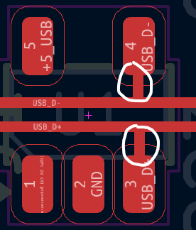
Make sure that differential pair net names end with
+and-orPandN.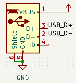
-
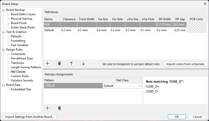
In PCB Editor open File → Board Setup and create a net class for differential pair nets. Specify differential pair (DP) width and gap from PCB manufacturer’s calculator or from some other calculator.
-
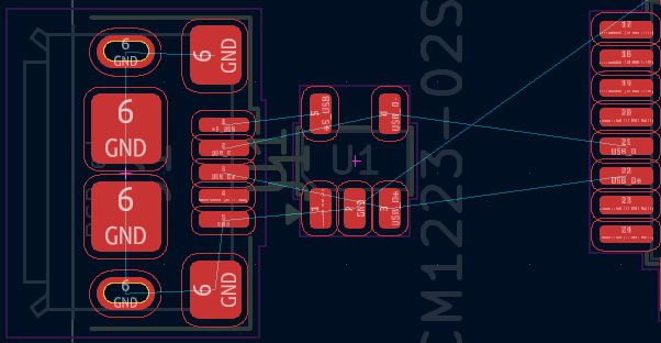
Position components so that the differential pair traces can be as straight as possible. If there are other components or traces close to the differential pair traces, try to move them further away.
-
Start routing by clicking Route Differential Pairs button or by pressing
6on keyboard.
KiCad documentation: https://docs.kicad.org/9.0/en/pcbnew/pcbnew.html#routing-differential-pairs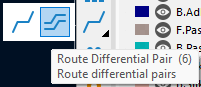
To reduce impedance discontinuities and intra-pair skew: try to avoid bends, avoid using vias if possible or reduce the amount of vias and keep traces as symmetrical as possible.
Some manual adjustments might be needed, which can be done by simply moving the tracks or rerouting segments of the tracks with Route Single Track ( hotkey
X) tool.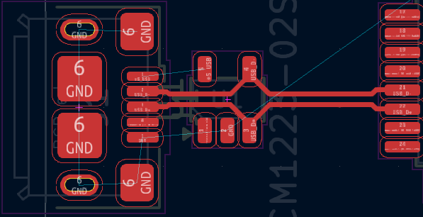
When connecting tracks to ESD protection component, the tracks should go straight to the ESD protection component (like on the image above) to avoid ESD propagating between narrow gaps between tracks.
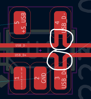
Stubs should be avoided in tracks as these will reduce ESD protection effectiveness and also cause signal reflections in general.