Altium Designer
Project
General
-
Press Space while moving objects to rotate them.
-
Press X while moving objects to mirror them in X axis.
-
Press Y while moving objects to mirror them in Y axis.
-
Drag from left to right to select objects that are fully inside the selection box.
-
Drag from right to left to select objects that are at least partially inside the selection box.
Creating components
Creating component footprint
-
Find a dimensional drawing for the component’s package. Usually package drawings are located at the end of the component’s datasheet.
-
Open *.PcbLib file.
-
Tools → IPC Compliant Footprint Wizard…
-
Select Component Type (for example PQFP which is used by the recommended microcontroller) and press Next.
-
Change Overall Dimensions based on the datasheet and press Next.
-
Change Pin Dimensions based on the datasheet and press Next.
-
Add Thermal Pad if necessary and press Next.
-
Use calculated values for Heel Spacing and press Next.
-
Use default values for Solder fillets and press Next.
-
Use calculated component tolerances and press Next.
-
Use Default Values for IPC tolerances and press Next.
-
Use calculated footprint values for Footprint Dimensions and press Next.
-
Silkscreen line width can be 0.2 mm. Press Next.
-
Use defaults for Courtyard, Assembly and Component Body Information and press Next.
-
Use suggested values for Footprint Description and press Next.
-
Select Current PcbLib File for Footprint Destination. Select Produce 3D/STEP model to create 3D model of the component. Also select Embedded. Press Finish.
-
Press Ctrl + S to save the PCB library.
Creating component symbol
-
Open *.SchLib file.
-
In Properties panel set
-
Design Item ID (for example STM32G431KBT6)
-
Designator (for example U?)
-
Comment (for example STM32G431KBT6)
-
-
Pins of the symbol can be placed individually with Place → Pin or in a bigger batch with Tools → Symbol Wizard…
-
Pin names can be found in the datasheet.
-
Try to arrange the symbol such that the center of symbol is at 0 coordinates.
-
Symbols typically have a rectangle in the middle of the symbols, which is created automatically by Symbol Wizard.
-
A rectangle can be placed with Place → Rectangle
-
If the rectangle is covering the pins, then it can be moved below the pins with selecting Edit → Move → Send To Back and clicking on the rectangle.
-
-
When the symbol is finished, then press Add Footprint
-
In the PCB Model window press Browse… and select the footprint created for the component.
-
-
Press Ctrl + S to save the Schematic library.
Schematic
Placing components
-
Open *.SchDoc file.
-
Open Components panel
-
Select *.SchLib from the dropdown.
-
Drag the component on the schematic or right click on it and select Place.
-
Symbols for some other components can be found from Manufacturer Part Search panel.
-
Symbols for power are available on the top toolbar.
PCB design
Importing schematic changes to PCB design
-
Open *.PcbDoc file.
-
Use Design → Import Changes From <your project name>.PrjPcb
-
Changing units
-
Press Q
-
Units can be checked in the bottom left corner.
-
Millimeters are recommended for the PCB.
-
Changing grid
-
In the schematic document:
-
Press G
-
Active grid is shown at the bottom left next to the coordinates.
-
It’s recommended to use 100 mil grid for components and wires as the symbols are created for that grid size. Sometimes it’s useful to use finer grid when creating schematic symbols or moving reference designators and component values.
-
-
In PCB layout document:
-
Press G and select suitable grid size from the list.
-
Good grid size for most of the layout is 0.1 mm. 0.025mm might work better for smaller components and thin tracks. 1mm grid is useful for changing board size.
-
Changing board size
-
Press 1
-
Select Design → Edit Board Shape
-
Press 2 to go back to PCB layout editing.
Hiding rooms
-
Press L to open View Configuration.
-
Open View Options tab.
-
Press on the eye icon next to the "Rooms".
Changing layer stackup
-
Go to https://jlcpcb.com/impedance for stackup descriptions.
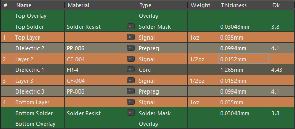
Recommended 4-layer stackup from JLCPCB is JLC04161H-3313. It costs the same as the default one (JLC04161H-7628), but has smaller distance between adjacent layers, which is helpful for reducing crosstalk.
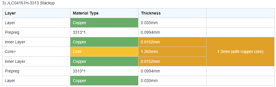 Figure 1. JLC04161H-3313 stackup with 1.6mm thickness, 1oz outer copper and 0.5oz inner copper weight
Dielectric constants for materials used by JLCPCB can be found here: https://jlcpcb.com/help/article/User-Guide-to-the-JLCPCB-Impedance-Calculator
-
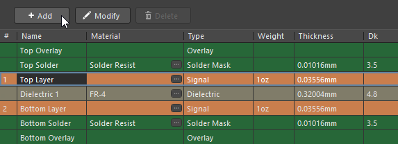
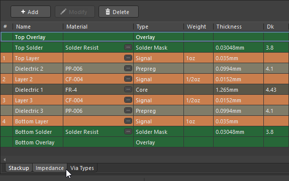
Open stackup editor with Design → Layer Stack Manager…
-
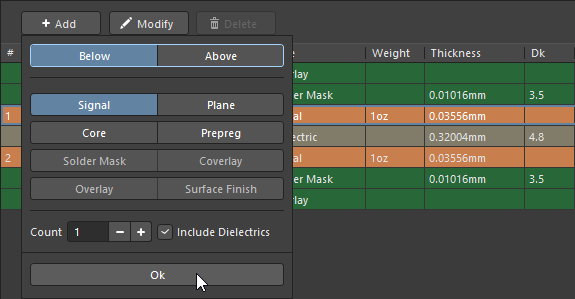
Select Top Layer and press Add.
-
Select Below, Signal and make sure that Include Dielectrics is selected. Press Ok.
-
Change Thickness and dielectric constant (Dk) values based on JLCPCB specifications. Rename Layer 1 and Layer 2 as Layer 2 and Layer 3. Change copper weight of inner layers to 1/2oz. Change Dielectric 1 type to Core.
Controlled impedance
Using Altium Designer’s impedance calculator
-
Open stackup editor with Design → Layer Stack Manager…
-
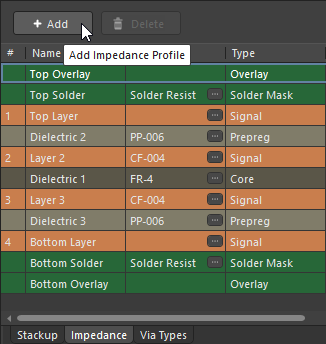
Press Add to create new impedance profile.
-
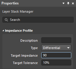
On Properties panel change Type to Differential and Target Impedance to 90. 90 Ohms is the differential impedance of USB differential pairs.
-
Change Trace Gap for each layer to 0.2mm. Can be narrower or wider if needed. Same differential impedance can be achieved with different trace widths and gaps. Also on Properties panel change Covering (C2) (Soldermask thickness above traces) to 0.6mil (0.01524mm). JLCPCB has specified soldermask thickness values on this page: https://jlcpcb.com/impedance.
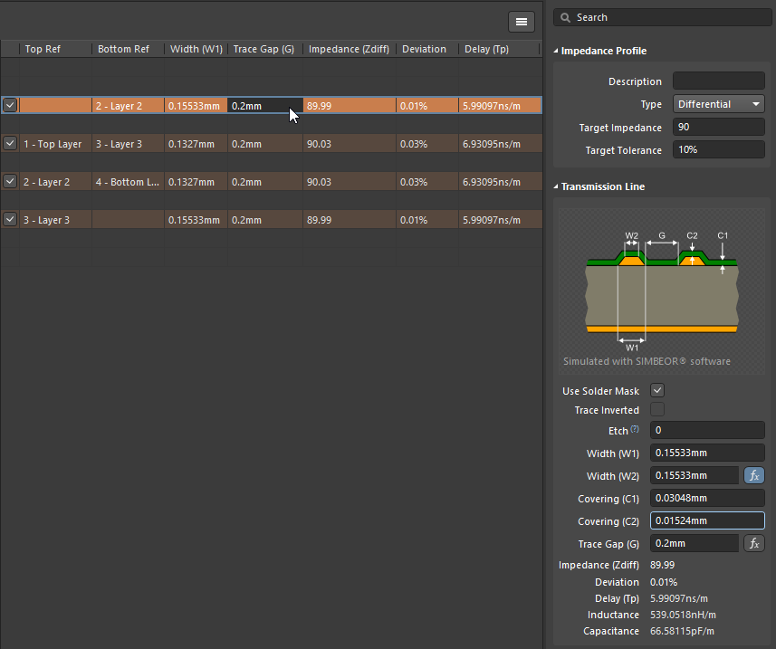
-
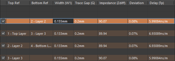
Manually round trace widths. This is not required, but sometimes useful on a dense board or if you like rounder numbers.
-
Save changes.
-
Open schematic (*.SchDoc).
-
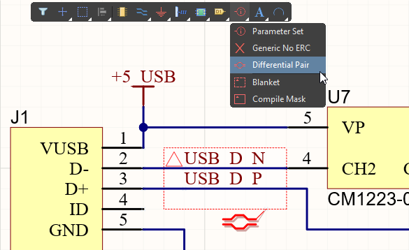
Add net labels to differential pair signals with _P suffix for positive signal and _N suffix for negative signal. It’s possible to specify different suffixes in Project Options, but there is probably no real need for that. Enclose net labels in a Blanket and add a Differential Pair directive so that it touches the blanket. It’s possible to add separate Differential Pair directive to both nets, but it’s easier to specify common parameters with a blanket.
-
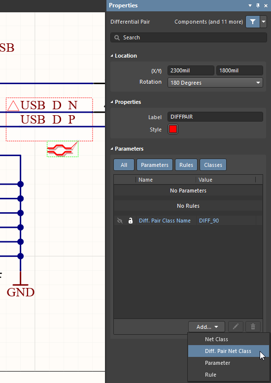
Select the Differential Pair directive and on the Properties panel add Diff. Pair Net Class named DIFF_90 for example.
-
Save changes.
-
Open *.PcbDoc.
-
Import schematic changes with Design → Import Changes From <your project name>.PrjPcb
-
Open Rules with Design → Rules…
-
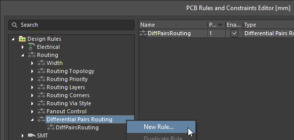
Right click on Differential Pairs Routing and select New Rule…
-
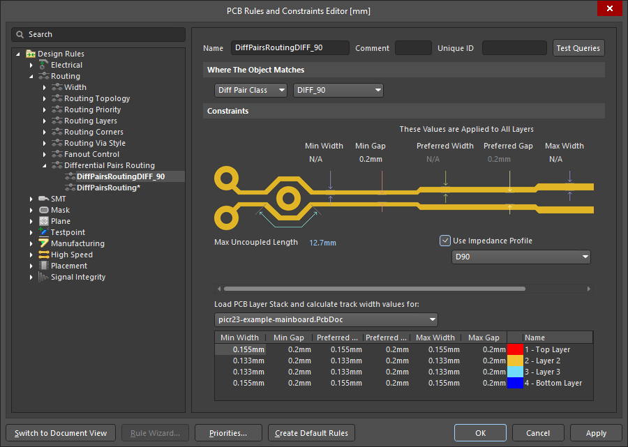
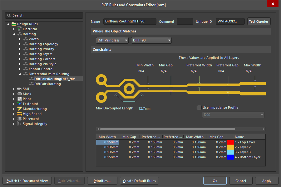
Name the rule as DiffPairsRoutingDIFF_90. Under Where The Object Matches select Diff Pair Class and DIFF_90. Activate Use Impedance Profile and select D90. Press OK to apply changes and close the rules.
Using manufacturer’s impedance calculator
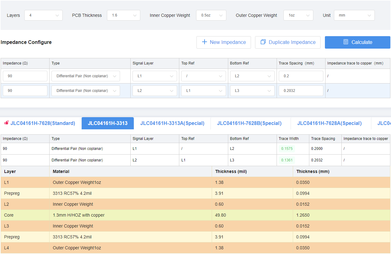
Another option, if a PCB manufacturer has an impedance calculation tool available, is to enter the calculated values manually to the rule. JLCPCB has an impedance calculator available here: https://jlcpcb.com/pcb-impedance-calculator/
-
Open the impedance calculator.
-
Change the input parameters and press Calculate. Calculated trace width on the outer layers for a 90-Ohm differential impedance with a 0.2mm gap and JLC04161H-3313 stackup is 0.1575mm:
-
Trace width and gap values can be used to define a differential pair routing rule.
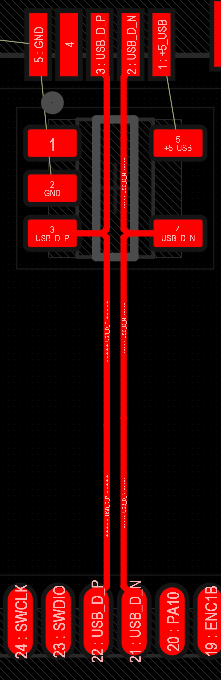
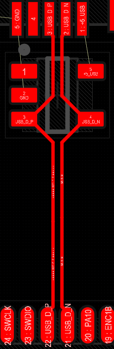
Routing differential pairs
-
Open *.PcbDoc
-
Position components so that the differential pair traces can be as straight as possible. If there are other components or traces close to the differential pair traces, try to move them further away.
-
Start routing with Route → Interactive Differential Pair Routing (U → I). To reduce impedance discontinuities and intra-pair skew: try to avoid bends, avoid using vias if possible or reduce the amount of vias and keep traces as symmetrical as possible.
-
If needed, adjust traces manually to reduce stub lengths. This can be done with regular routing (Route → Interactive Routing [Ctrl+W or U → T]) and some manual deleting and moving of the traces.
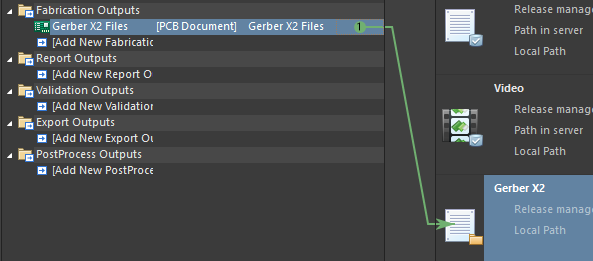
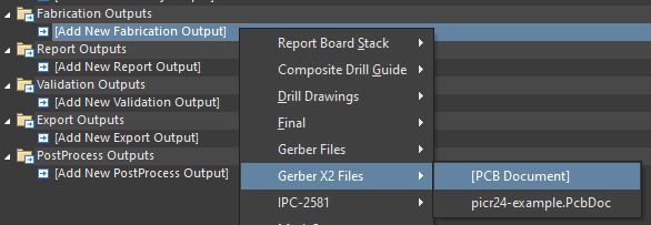
Generating Gerber X2 files
Add OutJob to project
-
Right click on *.PrjPcb and select Add New to Project → Output Job File.
-
Save *.OutJob file. It can have the same name as the project.
Add Gerber X2 output to OutJob
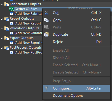
Click on [Add New Fabrication Output] and select Gerber X2 Files → [PCB Document].
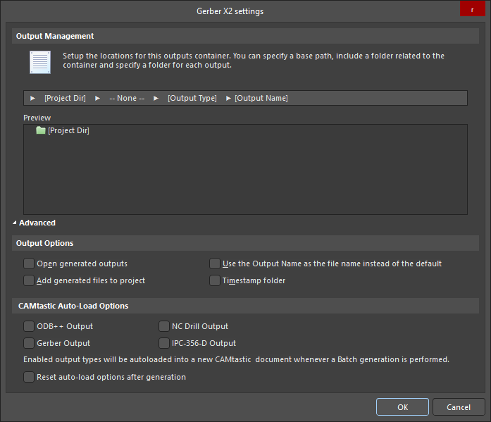
Configure Gerber X2 output
-
Double-click on Gerber X2 Files or right click and select Configure…
-
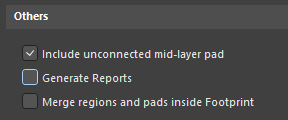
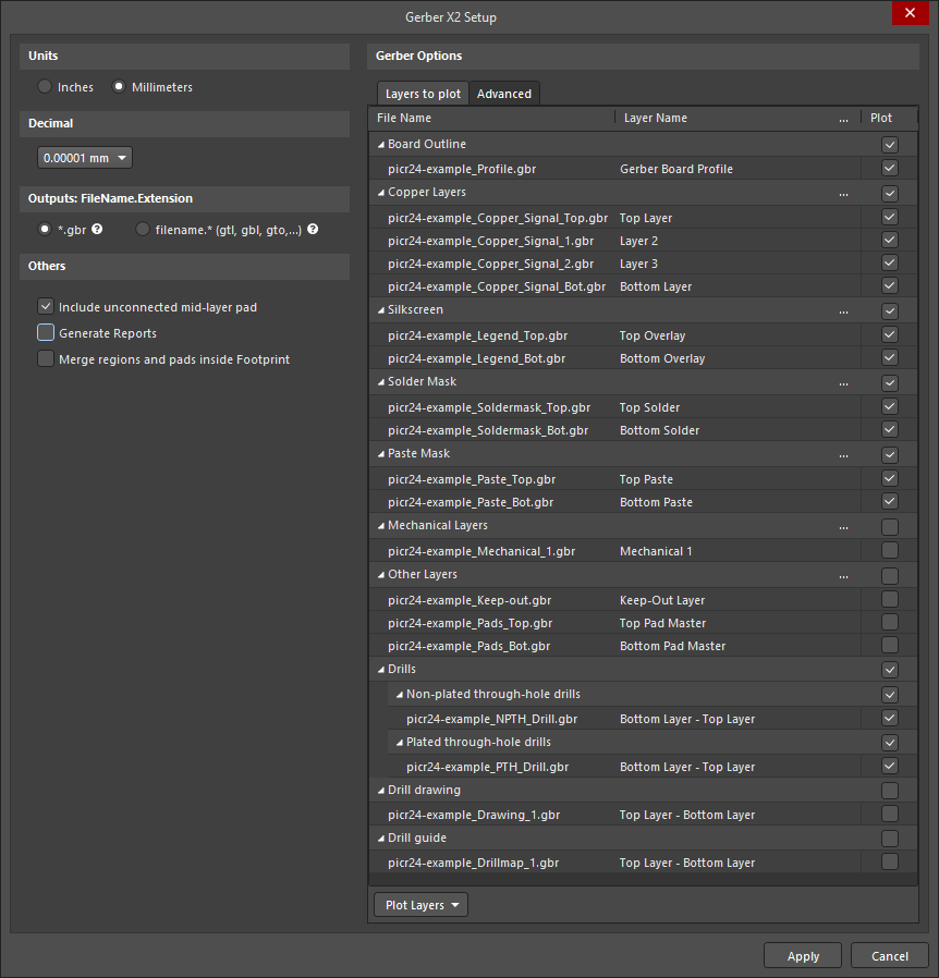
Untick Generate Reports.
-
Make sure that Plot column is ticked for Board Outline, Copper Layers, Silkscreen, Solder Mask and Drills. Paste Mask is optional. Paste Mask files are needed for creating solder paste stencils.
-
Press Apply.
Add New Output Container
-
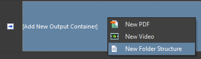
Click on [Add New Output Container] and select New Folder Structure.
-
Name it Gerber X2.
Change output container settings
-
Click on Change on output container.
-
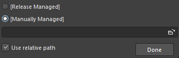
Click on [Release Managed], select [Manually Managed] and press Done.
-
Expand Advanced and untick "Open generated outputs" and "Add generated files to project".
-
Press OK.